- 您现在的位置:买卖IC网 > Sheet目录1990 > BU2365FV-E2 (Rohm Semiconductor)IC CLOCK GEN W/VCXO SSOP-B24
BU2365FV
Technical Note
3/16
www.rohm.com
2009.04- Rev.A
2009 ROHM Co., Ltd. All rights reserved.
Δf/f0
Hi-Z
L
H
0ppm
+60ppm
-60ppm
+15ppm
-15ppm
Vc
+30ppm
-30ppm
+45ppm
-45ppm
fH
fC
fL
※1 Period-Jitter 1
σ
This parameter represents standard deviation (=1
σ) on cycle distribution data at the time when the output clock cycles are
sampled 1000 times consecutively with the TDS7104 Digital Phosphor Oscilloscope of Tektronix Japan, Ltd.
※2 Period-Jitter MIN-MAX
This parameter represents a maximum distribution width on cycle distribution data at the time when the output clock cycles
are sampled 1000 times consecutively with the TDS7104 Digital Phosphor Oscilloscope of Tektronix Japan, Ltd.
※3 Output Lock-Time
This parameter represents elapsed time after power supply turns ON to reach a voltage of 3.0 V, after the system is
switched from Power-Down state to normal operation state, or after the output frequency is switched, until it is stabilized at
a specified frequency, respectively.
※4 Frequency stability
f0 : This parameter means an optimum frequency at T=25℃(27.000000 MHz), which represents a value of a single piece
of IC. Since no consideration is given to the stability of the crystal oscillator, it should be separately studied according to
the system in use.
※5 Frequency sensitivity/Frequency sensitivity linearity
These parameters represents that the frequency falls within the area shown in Fig. 2 in the control circuit of control voltage
shown in Fig. 1. It shows the value of IC itself. Since no consideration is given to the stability of the crystal oscillator, it
should be separately studied according to the system in use.
※Common – Recommended crystal oscillators
The electrical characteristics shown above have been all evaluated with the use of the crystal oscillator NX5032GA (Spec.
No. EXS00A-00278) manufactured by NIHON DEMPA KOGYO CO., LTD., under the conditions of Limiting resistance
Rd=30Ωand Crystal oscillator load CL=10pF. Consequently, in order to use the BU2365FV, the said crystal oscillator is
recommended.
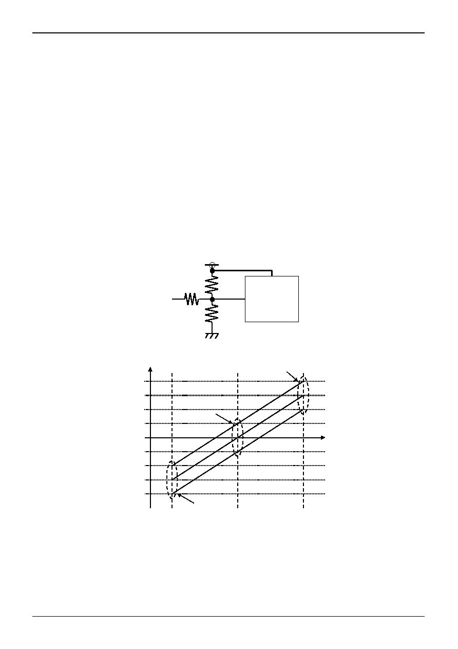
Fig.1 Control Circuit of Control Voltage
Frequency sensitivity dispersion range
:
fL = -45±15ppm, fC = 0±15ppm, fH = 45±15ppm
However, frequency sensitivity linearity
:
-10ppm≦(fH - fC) -( fC - fL) ≦+10ppm
Fig. 2 Frequency Sensitivity Dispersion Range
※6 Buffer skew
This parameter is only functional when the BUF_OUT1 and the BUF_OUT2 are driven at the same load capacitance.
R2
Vc
BU2365FV
R1:R2=1:0.875
R1
10Pin: VCTRL
9Pin
: VDD_V
发布紧急采购,3分钟左右您将得到回复。
相关PDF资料
BU2505FV-E2
IC DAC 10BIT 10-CHAN SSOP-B20
BU2508FV-E2
IC DAC 10BIT 4-CHAN SSOP14
BU3076HFV-TR
IC CLOCK GEN 1CH HVSOF6
CA3338AMZ96
IC DAC 8BIT 50MSPS R-R 16-SOIC
CDCR83DBQG4
IC DIRECT RAMBUS CLK GEN 24-QSOP
CDP68HC68T1M
IC RTC 32X8 NVSRAM CMOS 20-SOIC
CPLL66-1600-2200
IC VCO PLL/SYNTH 2.2GHZ SMD
CPLL66-2175-2175
IC VCO PLL/SYNTH 2175MHZ SMD
相关代理商/技术参数
BU2370FV
制造商:ROHM 制造商全称:Rohm 功能描述:VCO + phase comparator for TV
BU2373FV
制造商:ROHM 制造商全称:Rohm 功能描述:VCO & Phase-Detector for PLL System
BU2373FV_11
制造商:ROHM 制造商全称:Rohm 功能描述:High Performance VCOs for Image Sampling
BU-2373FV-E2
制造商:ROHM 制造商全称:Rohm 功能描述:High Performance VCOs for Image Sampling
BU2373FV-E2
功能描述:VCO振荡器 IMAGE SAMPL HI PERF VCO RoHS:否 制造商:Exar 封装 / 箱体:SOIC-14 频率:300 kHz 负载电容: 封装:Reel 电源电压:4.5 V to 20 V 尺寸:4 mm W x 8.75 mm L x 1.75 mm H 最小工作温度:0 C 最大工作温度:+ 70 C
BU2374FV
制造商:ROHM 制造商全称:Rohm 功能描述:VCO + phase comparator IC for PLL system
BU2374FV_1
制造商:ROHM 制造商全称:Rohm 功能描述:Silicon monolithic integrated circuit
BU2374FV-E2
功能描述:VCO振荡器 IMAGE SAMPL HI PERF VCO RoHS:否 制造商:Exar 封装 / 箱体:SOIC-14 频率:300 kHz 负载电容: 封装:Reel 电源电压:4.5 V to 20 V 尺寸:4 mm W x 8.75 mm L x 1.75 mm H 最小工作温度:0 C 最大工作温度:+ 70 C